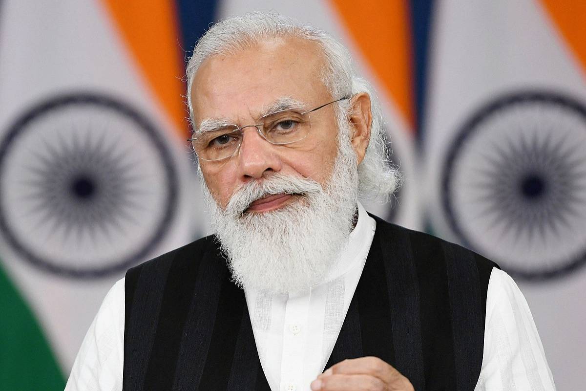
PM to visit Mauritius next week
Prime Minister Narendra Modi will be on a state visit to Mauritius on March 11-12 to attend the island's National Day celebrations as chief guest.
Due to supply-chain disruptions, many countries have announced financial incentives to companies for semiconductor manufacturing.

The Union Cabinet, chaired by Prime Minister Narendra Modi, today approved 50 per cent financial incentives for manufacturing of semiconductor fabs across technology nodes as well as for compound semiconductors, packaging, and other chip facilities.
Earlier, the government had announced 30-50 per cent incentives for different categories. However, the incentive has now been kept flat at 50 per cent for all categories. Also, so far the incentive was for 65 nm size, but now this restriction has been removed and all sizes will be covered.
Advertisement
Due to supply-chain disruptions, many countries have announced financial incentives to companies for semiconductor manufacturing. Therefore, India has tweaked the existing scheme to attract companies.
Advertisement
In December 2021, the Centre announced Rs 76000 crores for the development of the semiconductors and display manufacturing ecosystem in India.
Under the modified programme, uniform fiscal support of 50 per cent of the project cost shall be provided across all technology nodes for setting up of semiconductor fabs. Given the niche technology and nature of compound semiconductors and advanced packaging, the modified programme shall also provide fiscal support of 50 per cent of the capital expenditure in the pari-passu mode for setting up of compound semiconductors/silicon photonics/sensors/Discrete semiconductors fabs and ATMP/OSAT.
The programme has attracted many global semiconductor players for setting up fabs in India. The modified programme, will expedite investments in semiconductor and display manufacturing in India. On the basis of discussion with potential investors, it is expected that work on setting up the first semiconductor facility will commence soon.
An advisory committee comprising global experts from industry and academia was constituted to advise the India Semiconductor Mission – the nodal agency for the Programme for the development of semiconductors and the display manufacturing ecosystem in India.
The advisory panel has unanimously recommended uniform support for all technology nodes of silicon semiconductor fabs/Silicon Photonics/Sensors/Discrete Semiconductor Fabs and ATMP/OSAT, which has been accepted by the government. The technology nodes of 45nm and above have high demand which is inter-alia driven by automotive, power, and telecom applications. Moreover, this segment constitutes around 50 per cent of the total semiconductor market.
Advertisement